

 LED
LED

 LCD
LCD






Product Description
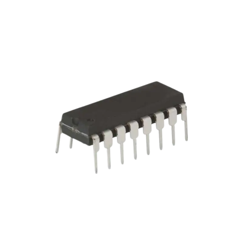
The 74194 4-Bit Bidirectional Universal Shift Register IC is a high-speed logic integrated circuit designed for flexible data storage, manipulation, and serial-parallel conversion in digital computing and automation systems. Featuring four distinct operational modes—Parallel Load, Shift Right, Shift Left, and Hold (Do Nothing)—this IC offers complete control over 4-bit data vectors on every positive edge of the clock signal.
Engineered with asynchronous direct clear overrides and individual parallel data inputs and outputs (QA through QD), the 74194 allows seamless bi-directional data transfers across digital buses. Housed in a standard 16-pin DIP package, it operates on a standard 5V DC supply and connects directly to 5V TTL and CMOS logic levels. It is an essential component for building shift registers, ring counters, sequence generators, ALU data buffers, and digital logic training kits with microcontrollers like Arduino, STM32, or discrete TTL setups.
⚠️ Operating Mode Setup Tip: The operational mode of the 74194 is determined by the state of control pins S0 and S1 on the rising edge of the clock (CLK). Ensure that S0 and S1 logic levels are stable before triggering the clock edge to prevent unexpected mode transitions. Taking the Clear (CLR) pin LOW resets all internal flip-flops to LOW asynchronously, regardless of clock or control inputs.
Technical & Logic Architecture
This universal shift register provides complete data routing flexibility:
Four-Mode Control Logic: Selectable operations via mode control inputs S0 and S1 (00 = Hold, 01 = Shift Right, 10 = Shift Left, 11 = Parallel Load).
Bi-Directional Serial Inputs: Dedicated Serial Shift-Right (SR) and Serial Shift-Left (SL) inputs for cascade expansion.
Asynchronous Master Clear: Low-active CLR input to instantly reset all four output flip-flops to zero.
Breadboard-Friendly Package: Standard 16-pin Dual In-Line Package (DIP-16) for easy insertion into breadboards and IC sockets.
74194 Truth Table (Function Table)
| Inputs: Clear (CLR) | Inputs: Mode S1 | Inputs: Mode S0 | Inputs: Clock (CLK) | Inputs: Serial Shift-Right (SR) | Inputs: Serial Shift-Left (SL) | Inputs: Parallel Inputs (A, B, C, D) | Outputs: QA | Outputs: QB | Outputs: QC | Outputs: QD | Operating Mode / Function |
| L | X | X | X | X | X | X | L | L | L | L | Asynchronous Clear (Reset) |
| H | L | L | X | X | X | X | QA0 | QB0 | QC0 | QD0 | Hold (No Change) |
| H | H | H | Rising Edge | X | X | a, b, c, d | a | b | c | d | Parallel Load |
| H | L | H | Rising Edge | H | X | X | H | QAn | QBn | QCn | Shift Right (Serial Input = HIGH) |
| H | L | H | Rising Edge | L | X | X | L | QAn | QBn | QCn | Shift Right (Serial Input = LOW) |
| H | H | L | Rising Edge | X | H | X | QBn | QCn | QDn | H | Shift Left (Serial Input = HIGH) |
| H | H | L | Rising Edge | X | L | X | QBn | QCn | QDn | L | Shift Left (Serial Input = LOW) |
Key Terms for Truth Table:
H: High Voltage Level (Logic 1)
L: Low Voltage Level (Logic 0)
X: Don’t Care (Can be High or Low)
Rising Edge: Low-to-High transition of the Clock signal
QA0, QB0, QC0, QD0: Output levels before the indicated input conditions were established
QAn, QBn, QCn, QDn: Output levels of QA, QB, QC, or QD respectively before the most recent clock pulse
74194 Pinout Description & Logic Functions

Pin 1 – CLR (Clear): Master Reset Input (Active LOW). Driving this pin LOW forces all outputs (QA to QD) to LOW asynchronously, regardless of Clock or Mode inputs.
Pin 2 – SR (Shift Right Serial Input): Serial data input used during Shift Right operations (when S1 = LOW, S0 = HIGH).
Pin 3 – A (Parallel Input A): Data input line for parallel loading into internal Flip-Flop A.
Pin 4 – B (Parallel Input B): Data input line for parallel loading into internal Flip-Flop B.
Pin 5 – C (Parallel Input C): Data input line for parallel loading into internal Flip-Flop C.
Pin 6 – D (Parallel Input D): Data input line for parallel loading into internal Flip-Flop D.
Pin 7 – SL (Shift Left Serial Input): Serial data input used during Shift Left operations (when S1 = HIGH, S0 = LOW).
Pin 8 – GND: Ground reference pin (0V).
Pin 9 – S0 (Mode Select 0): Mode control pin 0. Combined with S1 to set operational state.
Pin 10 – S1 (Mode Select 1): Mode control pin 1. Combined with S0 to set operational state.
Pin 11 – CLK (Clock Input): Trigger clock pin. Operations occur on the Low-to-High (Rising Edge) transition.
Pin 12 – QD (Parallel Output D): Digital output of the 4th bit position.
Pin 13 – QC (Parallel Output C): Digital output of the 3rd bit position.
Pin 14 – QB (Parallel Output B): Digital output of the 2nd bit position.
Pin 15 – QA (Parallel Output A): Digital output of the 1st bit position.
Pin 16 – VCC: Power supply input pin (+5V DC nominal).
Operating Modes Summary
Parallel Load (S1 = HIGH, S0 = HIGH): Transfers inputs A, B, C, and D simultaneously to outputs QA, QB, QC, and QD on the rising clock edge.
Shift Right (S1 = LOW, S0 = HIGH): Shifts data from QA toward QD. Serial data enters via the SR pin into QA on the rising clock edge.
Shift Left (S1 = HIGH, S0 = LOW): Shifts data from QD toward QA. Serial data enters via the SL pin into QD on the rising clock edge.
Hold / Do Nothing (S1 = LOW, S0 = LOW): Clock pulses are inhibited, maintaining current output states without change.
Applications
Data Format Conversion: Converting parallel bus data to serial transmission channels (and vice versa).
Sequence & Pattern Generators: Constructing Johnsons counters, ring counters, and automated LED chasers.
ALU Data Buffering: Storing and shifting binary numbers during arithmetic operations in custom digital processors.
Technical Specifications
| Parameter | Value / Specification |
| Logic IC Family | 74xx Series TTL / High-Speed CMOS |
| Supply Voltage (VCC) | 4.75V to 5.25V DC (Nominal 5V) |
| Bit Capacity | 4 Bits |
| Operational Modes | Hold, Shift Right, Shift Left, Parallel Load |
| Package Type | DIP-16 (16-Pin Through-Hole) |
| Operating Temperature | 0°C to 70°C |
What’s in the Box
1 x 74194 4-Bit Bidirectional Universal Shift Register IC (DIP-16).
Everything you need for your next project is now available with guaranteed quality and fast shipping across Egypt.. Order now from Pro Tronix!
🛠️ Complete Your Breadboard Setup
To quickly wire and test the 74194 Universal Shift Register IC without soldering, make sure to check out our collection of breadboards, prototype boards, and jumper wires:
Breadboards & Prototype PCBs: Explore our full range of solderless breadboards and prototyping boards for easy circuit assembly: Pro Tronix Breadboards & PCBs
Jumper Wires & Connecting Cables: Grab high-quality male-to-male and male-to-female jumper wires to connect your IC pins to power and signal lines: Pro Tronix Wires & Cables Collection
